Transistor
A transistor is a fundamental electronic component that plays a key role in amplifying and switching electrical signals. It is widely used in numerous electronic devices such as computers, televisions, mobile phones, radios, etc. (a processor can contain billions of them at nanometer-scale dimensions). The transistor is composed of three layers of semiconductor materials: N-type (negative), P-type (positive), and again N-type (negative) or vice versa, thus forming two PN junctions. Transistors can be divided into two main types: the bipolar junction transistor (BJT) and the field-effect transistor (FET).
Refer to the corresponding images and symbols below:
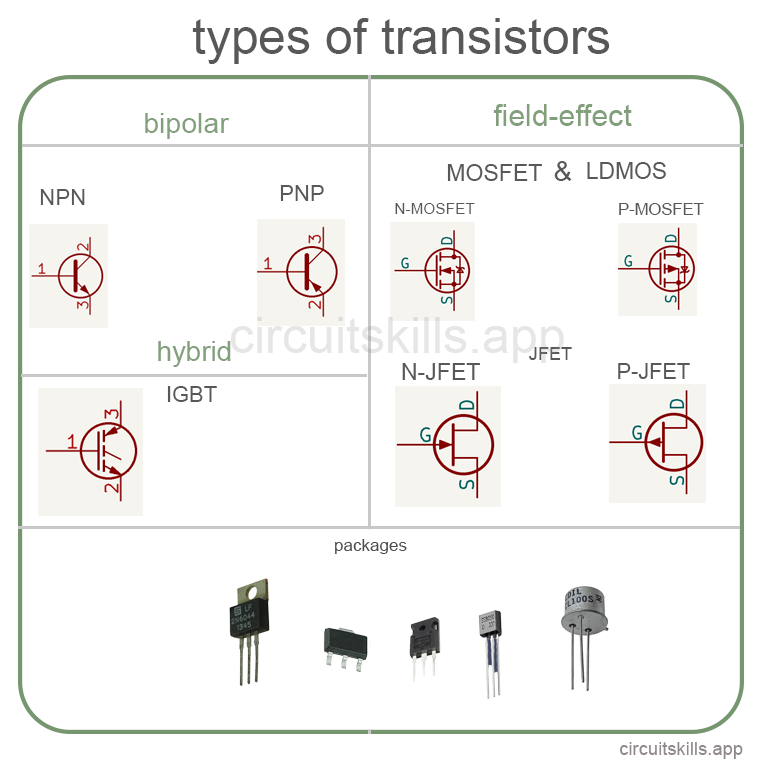
Bipolar (BJT - Bipolar Junction Transistor)
A bipolar transistor is an electronic component with three terminals (emitter, base, collector) consisting of three doped semiconductor layers (NPN or PNP). It functions as a switch or current amplifier, where a small current applied to the base controls a larger current between the emitter and collector. There are two main types: NPN and PNP, which differ in voltage polarity and current direction.
The Concept of Gain
Refers to its ability to amplify an electrical signal, whether in current, voltage, or power. It is a fundamental parameter that quantifies the transistor's efficiency in increasing the amplitude (height/voltage) of a signal.
There are primarily two types of gain for a bipolar transistor, commonly used in the common-emitter configuration, which is the most typical setup for amplification:
-
Current Gain (β or hFE)
- This is the ratio between the collector current (Ic), the output current, and the base current (Ib), the input current.
- It indicates how many times the transistor amplifies the current injected into its base to produce a larger current in the collector.
- A typical β value ranges between 50 and 300 for small-signal transistors but may differ for power transistors or specific configurations like Darlington pairs.
- Formula: β = Ic / Ib
-
Voltage Gain (Av)
- In an amplifier circuit using a bipolar transistor, the voltage gain is the ratio between the output voltage (at the collector) and the input voltage (at the base).
- The value of this gain depends on the circuit configuration (resistors used, etc.) and the transistor's characteristics.
In summary, the gain of a bipolar transistor is a factor that indicates how many times the input signal is multiplied to obtain the output signal. A high gain means greater amplification. This parameter is crucial for determining the performance of an amplifier circuit based on a bipolar transistor. It is important to note that a transistor's gain is not constant and can vary depending on the collector current, collector-emitter voltage, temperature, and signal frequency.
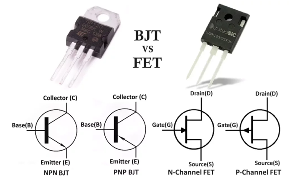
Field-Effect (FET - Field-Effect Transistor)
A field-effect transistor is an electronic component with three terminals (source, drain, gate) where the current between the source and drain is controlled by an electric field applied to the gate. Unlike bipolar transistors, which are current-controlled, FETs are voltage-controlled, giving them a very high input impedance. There are two main types: JFET (Junction FET) and MOSFET (Metal-Oxide-Semiconductor FET), each with subcategories (N-channel or P-channel, enhancement or depletion mode for MOSFETs). In short, it is a switch or amplifier controlled by voltage.
1. JFET (Junction Field-Effect Transistor)
A JFET is a type of field-effect transistor where conduction between the source and drain is controlled by a voltage applied to the gate.
Key Points:
- Operation by electric field: Unlike current-controlled bipolar transistors, the JFET uses an electric field to modulate the width of a conductive channel between the source and drain.
- PN junction: The gate is formed by a PN junction with the conductive channel. Applying a reverse voltage to this junction creates a depletion region that narrows the channel, reducing current flow between the source and drain.
- Voltage control: A small variation in gate voltage can cause a large variation in drain-source current.
- High input impedance: Due to the reverse-biased PN junction, the JFET exhibits very high input impedance at the gate, meaning it draws minimal current from the control circuit.
- Two types: N-channel and P-channel JFETs, depending on the semiconductor type used for the conductive channel.
- Applications: Used in amplifiers, switches, and high-input-impedance circuits.
2. MOSFET (Metal-Oxide-Semiconductor FET)
A MOSFET is another type of field-effect transistor, but it differs from the JFET in how the gate controls current.
Key Points:
- Insulated gate: The defining feature of a MOSFET is that its gate is insulated from the conductive channel by a thin oxide layer (typically silicon dioxide, SiO₂). This insulation gives it the name "Metal-Oxide-Semiconductor."
- Electric field control (no gate current): Applying a voltage to the gate creates an electric field across the oxide. This field induces (or repels) charge carriers (electrons or holes) in the underlying channel, modulating its conductivity and thus the current between the source and drain. Thanks to the gate insulation, the gate current is practically zero.
- Two operating modes:
- Enhancement Mode: No channel exists at zero gate voltage. Applying an appropriate gate voltage creates a conductive channel. This is the most common type used as a switch.
- Depletion Mode: A channel already exists at zero gate voltage. Applying an appropriate gate voltage (of opposite polarity) reduces the channel's conductivity by repelling charge carriers.
- Two channel types: Like JFETs, MOSFETs come in N-channel (NMOS) and P-channel (PMOS) varieties, depending on the majority charge carriers in the channel.
- Extremely high input impedance: The gate's oxide insulation gives MOSFETs even higher input impedance than JFETs, typically in the range of several gigaohms.
- Applications: MOSFETs are ubiquitous in digital electronics (microprocessors, memory), power supplies, amplification, and power switching.
RF Power FET (LDMOS - Laterally Diffused MOSFET)
An LDMOS is a specialized high-power RF MOSFET with a lateral structure for better voltage handling.
Key Points:
- Lateral structure: Unlike conventional power MOSFETs with vertical structures, LDMOS transistors have a planar (lateral) design. This configuration optimizes electric field distribution and improves voltage tolerance.
- Double diffusion: The channel is formed through two impurity diffusion steps, allowing precise control of its length and doping, optimizing RF performance and breakdown voltage.
- Primary applications: RF power amplifiers for cellular base stations, radar, radio/TV broadcasting, industrial RF/microwave heating, and some high-power audio applications.
Hybrid (IGBT - Insulated Gate Bipolar Transistor)
The IGBT is a hybrid transistor combining a MOSFET (input) and a bipolar transistor (output). It is controlled by the gate-emitter voltage (like a MOSFET) but has the conduction characteristics (between collector and emitter) of a bipolar transistor.
Advantages:
- Low gate drive power (MOSFET-like).
- Lower conduction losses (for a given chip size) than bipolar transistors.
- Can handle much higher voltages than MOSFETs.
Applications:
- Power electronics (inverters, motor drives, electric vehicles).
Summary Table
See other components: