Understanding the Common Collector Amplifier: The Complete Guide
Among the three major BJT amplifier configurations, the Common Collector Amplifier, also known as the Emitter Follower, is widely used thanks to its high input impedance, low output impedance, and excellent buffering capability. Whether you are designing audio stages, sensors, or interface circuits, mastering this configuration is essential.
What you'll learn
What is a Common Collector Amplifier?
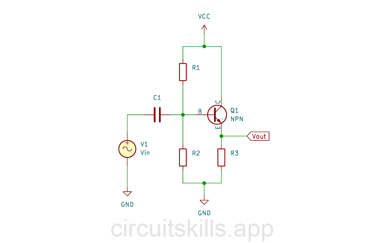
The Common Collector amplifier gets its name because the collector terminal is the point shared between the input and the output. The output is taken from the emitter, which “follows” the input voltage, hence the name Emitter Follower.
This configuration provides unity voltage gain (close to 1) but delivers high current gain and excellent impedance matching. It is ideal whenever a circuit requires driving a low-impedance load from a high-impedance source.
The Emitter Follower and Biasing
Like any transistor amplifier, the emitter follower requires correct biasing to operate in its linear region. The goal is to set the transistor so that the output can reproduce the entire AC signal without distortion.
The biasing ensures the transistor stays in the active region, avoiding cutoff and saturation. This stability is crucial to prevent signal clipping and to guarantee a faithful reproduction of the input waveform.
The Role of the Load Line
The DC load line helps us visualize how the transistor behaves between its ON and OFF states. By selecting a proper Q-point, usually centered on the load line, we ensure maximum output swing without distortion.
Because the emitter follower amplifies current rather than voltage, the Q-point selection is essential for ensuring linearity and thermal stability.
Circuit Analysis: Components and Formulas
A typical Common Collector amplifier uses voltage divider biasing to set the base voltage. Here are the essential elements:
1. The Voltage Divider (R1 and R2)
These resistors create the base voltage (VB). This ensures the transistor remains in active mode during the whole signal cycle.
VB =VCC×(R2 / (R1 + R2))
2. The Emitter Resistor (RE) = R3
The resistor RE stabilizes the current and defines the output voltage. The emitter voltage is:
VE = VB − 0.7V
The emitter current is then calculated using Ohm’s law:
IE = VE/ RE
3. Coupling and Bypass Capacitors
Cin (C1) and Cout (Coupling Capacitors): They allow AC signals to pass while blocking DC components, preventing shifts in bias from previous or next stages.
CE (Bypass Capacitor): Placed in parallel with RE. It increases AC gain by reducing the AC emitter resistance, enhancing current amplification.
Voltage Gain and Impedance
Unlike the Common Emitter amplifier, the Common Collector does not invert the signal. The output is almost in phase with the input.
While the voltage gain is slightly less than 1, the configuration provides:
- Very high input impedance
- Very low output impedance
- Excellent current amplification
Voltage Gain Formula (AV)
The voltage gain is the ratio between output voltage (Vout) and input voltage (Vin).
With the bypass capacitor present, the gain is approximately:
AV ≈ r'e / (r'e + RE)
(Since RE dominates, the gain is slightly below 1.)
Practical Exercises
Test your understanding with these exercises.
Exercise 1: DC Analysis
Data:
- VCC = 12V
- R1 = 47 kΩ, R2 = 10 kΩ
- RE = 1 kΩ
- VBE = 0.7V (Silicon Transistor)
Question:
Calculate the base voltage (VB) and the emitter current (IE).
Answer:
Calculate VB (Voltage Divider):
VB = 12V × (10kΩ / (47kΩ + 10kΩ)) = 12V × 0.175 =2.1V
Calculate VE:
VE = VB − 0.7V = 2.1V − 0.7V = 1.4V
Calculate IE:
IE = VE / RE = 1.4V / 1000Ω = 1.4 mA
Exercise 2: Voltage Gain Calculation
Data:
- Using the previous result: IE ≈ 1.4 mA.
- Internal dynamic emitter resistance r′e = 25mV / IE.
- RE = 1 kΩ.
Question:
Calculate the voltage gain Av.
Answer:
Calculate r′e:
r′e = 25mV / 1.4mA ≈ 17.8 Ω
Calculate Gain Av:
Av ≈ r′e / (r′e + RE) = 17.8Ω / (17.8Ω + 1000Ω) ≈ 0.017
The amplifier provides a voltage gain slightly below 1 but a very high current gain, which is its key advantage.
Summary
The Common Collector Amplifier (Emitter Follower) plays a crucial role in analog design. Here is what you should remember:
- Configuration: The collector is common to input and output.
- Impedance: High input impedance, low output impedance.
- Gain: Voltage gain close to 1, strong current gain.
- Phase: Output signal is in phase with input.
- Applications: Buffering, impedance matching, and driving low-resistance loads.
Need Clarification?(-10/req)
AIcredits:0